

Advanced packaging has become the next battleground in semiconductor performance as chipmakers shift from 2D to 3D architectures.
Advanced packaging has become the next battleground in semiconductor performance as chipmakers shift from 2D to 3D architectures.
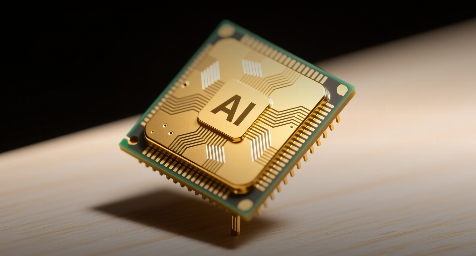
Qnity Electronics joined imec's research program to accelerate advanced chip packaging, betting that chiplets and 3D stacking will define semiconductor performance as AI workloads push traditional designs to their limits.
"Advanced packaging is becoming one of the most critical frontiers for performance, efficiency and scale," Randy King, Chief Technology Officer at Qnity, said.
Qnity's platform spans the full packaging chain from front-end to back-end materials, including patterning, planarization, metallization, interconnect technologies and thermal management. The company is targeting chiplets (modular dies that replace monolithic chips), high-bandwidth memory, wafer-level packaging and heterogeneous integration — technologies that stack components vertically rather than spreading them across a 2D plane. Through its membership in imec's research program, Qnity gains access to the Belgian lab's infrastructure, experts and network of industry and academic partners.
The investment positions Qnity to capture a larger share of the advanced packaging market as chipmakers like Nvidia and AMD increasingly rely on packaging innovation to boost performance when traditional node shrinks deliver diminishing returns. Qnity's materials expertise across the packaging stack gives it a differentiated position versus pure-play packaging foundries.
The semiconductor industry's shift toward heterogeneous integration — combining multiple specialized dies in a single package — has turned packaging from an afterthought into a critical performance lever. Nvidia's H100 and B200 GPUs use TSMC's CoWoS (chip-on-wafer-on-substrate) packaging to stack HBM memory alongside the compute die, enabling memory bandwidth exceeding 3 terabytes per second. Without such packaging, the performance gains from each new process node would be increasingly bottlenecked by data movement between chips.
Qnity's approach differs from that of TSMC and other foundries by focusing on the materials layer — the chemicals, slurries and films that enable these complex packaging architectures. The company's portfolio includes materials for patterning (defining circuit features), planarization (flattening surfaces between layers), metallization (creating conductive pathways) and thermal management (dissipating heat from stacked dies). Each step becomes more challenging as the number of stacked layers increases.
The partnership with imec, a leading semiconductor research organization based in Leuven, Belgium, gives Qnity early access to emerging packaging roadmaps. Imec's research programs span process technology, design and packaging, making it one of the few institutions that can validate materials at scale before they enter commercial production. For Qnity, this means shorter development cycles and the ability to co-design materials alongside the chipmakers who will use them.
Qnity shares, trading on the New York Stock Exchange under ticker Q, have not disclosed the financial terms of the imec partnership or the total investment in packaging research and development. The broader advanced packaging market is projected to reach $78 billion by 2030, growing at a compound annual rate of about 10 percent, according to industry estimates. Qnity's ability to capture share will depend on how quickly its materials are adopted in high-volume manufacturing for AI accelerators and HPC processors.
This article is for informational purposes only and does not constitute investment advice.
