

Key Takeaways: Synopsys has become the first company to verify an HBM4 IP test chip, running at 9.2 Gbps with real HBM DRAM.
Key Takeaways: Synopsys has become the first company to verify an HBM4 IP test chip, running at 9.2 Gbps with real HBM DRAM.
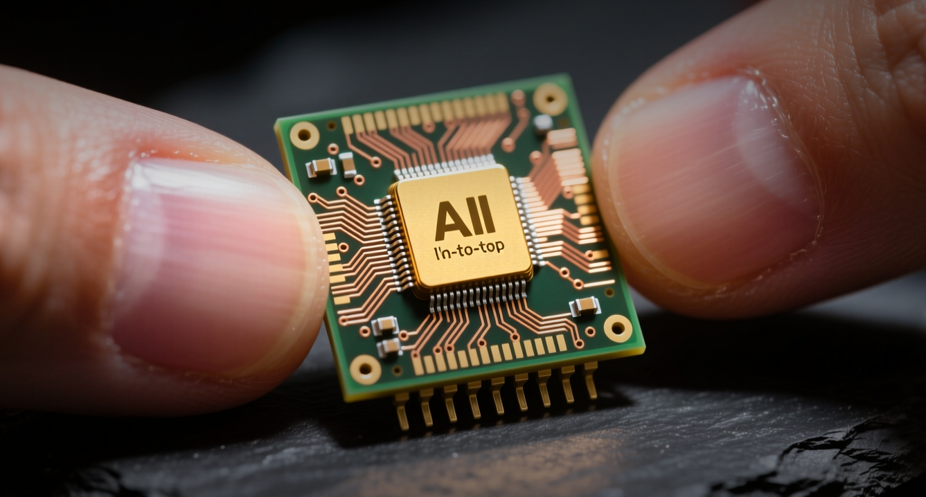
Synopsys verified the world's first HBM4 IP test chip at 9.2 Gbps, completing interconnect validation against real HBM DRAM and moving ahead of Cadence in the memory interface IP race.
"Now we are preparing for HBM 5 technology, which will increase that stack height to 24, which means even more data going back and forth," Faisal Goriawalla, director of product management at Synopsys, said. "As the pitch between these signals is squeezed, you have electrical interference challenges such as the victim aggressor situation."
The test chip verification covers the PHY, interface architecture, signal transmission, and compatibility with real HBM DRAM. Multiple customers have already adopted Synopsys' HBM4 IP solution. HBM4 stacks 16 DRAM chiplets and marks the transition to hybrid bonding, where copper-to-copper connections replace traditional microbumps.
The milestone positions Synopsys to capture a larger share of the memory interface IP market as AI-driven demand for high-bandwidth memory accelerates. HBM4's shift to custom logic base dies and hybrid bonding creates new IP opportunities across the AI accelerator supply chain.
HBM4 represents a significant architectural shift from its predecessor. HBM3 stacks 12 or more DRAM chiplets atop a silicon interposer, interconnected by finely spaced through-silicon vias (TSVs) and connected by microbumps. HBM4 increases the stack to 16 DRAMs and transitions to hybrid bonding — a copper-to-copper connection method that eliminates solder bumps entirely, enabling tighter pitch and higher bandwidth.
The transition to hybrid bonding for HBM4 processes puts more focus on ensuring the quality of each interconnect bond. "As we're stacking these devices, the coplanarity, the warpage, the bonding processes, and everything that we're doing to make these individual bonds from a C4 bump to a copper-to-copper bump or a die-to-die connection — each one of these bonds is critical," said Jack Lewis, CTO of Modus Test.
HBM4's Custom Logic Base Die Opens New IP Opportunities
A key differentiator of HBM4 is the option of a custom logic base die that replaces the DRAM-built controller die of previous generations. Custom HBM allows AI accelerator or GPU designers to optimize the memory stack for specific workloads, particularly important for AI training and inference where performance is more often bandwidth-limited than compute-limited.
"Custom HBM gives SOC designers tremendous flexibility to configure the logic base die the way they want," said Goriawalla. "If you are in a data center AI training environment where latency and throughput are very important factors, you can configure your HBM controller for those goals. But if you are in an AI inference type of application, where area and power are bigger concerns, then you can configure the HBM controller and logic differently."
The additional logic circuitry in custom HBM means more opportunity to use on-die monitors on the base die to help detect timing margin problems. "We look at the SoCs and HBMs as a system because there's interaction between the two," said Noam Brousard, vice president of solutions engineering at proteanTecs. "A lot of traffic coming in from the HBM might cause a current surge, which leads to a voltage droop."
Testing Complexity Grows With Stack Height
HBM testing has become a major bottleneck due to the complexity of test program development. "Creating the specialized fault models and test algorithms necessary for detecting defects in TSVs, microbumps, and inter-die interfaces is an intricate process requiring deep expertise," said Quoc Phan, technology enablement manager of 3DIC DFT and yield at Siemens EDA.
Interconnect bump pitch between DRAMs in HBM is now so tight — below 40 microns, with 20 to 25 micron microbumps — that it has become nearly impossible to probe the microbumps directly. Engineers are increasingly dependent on built-in self-test (BiST) options, embedded monitors and sensors, and redundancy and repair mechanisms to ensure higher interconnect yield.
The competitive stakes are high. HBM is the proving ground for 3D stack testing, DFT, and reliability, with SK hynix, Samsung, and Micron as the primary HBM manufacturers. Synopsys' early HBM4 IP verification gives it a first-mover advantage in the IP market that serves these manufacturers and the AI accelerator designers who integrate HBM into their systems.
For investors, the question is whether Synopsys can convert this technical milestone into sustained IP revenue growth. The company's semiconductor IP business competes directly with Cadence in the memory interface IP space, and HBM4's complexity — 16 DRAM stacks, hybrid bonding, custom logic base dies — creates a larger addressable market for IP solutions. As AI accelerators from Nvidia, AMD, and others continue to push memory bandwidth limits, the demand for verified HBM4 IP is expected to grow through the current product cycle.
This article is for informational purposes only and does not constitute investment advice.
