

Intel's partnership with Lens Technology to develop glass-based chip packaging targets a critical bottleneck in AI computing: the physical limits of organic substrates.
Intel's partnership with Lens Technology to develop glass-based chip packaging targets a critical bottleneck in AI computing: the physical limits of organic substrates.
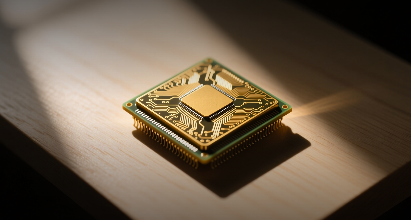
Intel Corp. partnered with Lens Technology to develop glass-based semiconductor packaging, aiming to improve interconnect density and thermal performance for AI chips as demand for advanced packaging outstrips supply.
"Intel is well positioned to benefit from this strong, sustained demand with three strategically important assets: our X86 CPU franchise, our advanced packaging technology and our vast wafer foundry network," Lip-Bu Tan, Intel's chief executive officer, said on the company's July 23 earnings call.
Intel will contribute its semiconductor architecture and advanced packaging expertise while Lens Technology brings glass material processing, laser manufacturing and mass-production capabilities, the companies said. Financial terms were not disclosed. The partnership could extend into AI PC components, data center server cooling and edge computing hardware.
The collaboration positions Intel to accelerate glass substrate adoption — a technology that offers better thermal and mechanical properties than organic substrates for high-performance AI chips — as it competes with Taiwan Semiconductor Manufacturing Co. and Samsung Electronics Co. in the advanced packaging market. Intel's foundry revenue rose 31% year-over-year to $5.8 billion in the second quarter, with Intel 18A yields running ahead of expectations.
Glass substrates replace the organic laminate used in conventional chip packaging, allowing finer line widths and greater dimensional stability under heat. For AI accelerators that consume hundreds of watts, the improved thermal management could enable higher clock speeds or denser transistor packing without reliability trade-offs. Lens Technology, a major supplier of glass components to Apple Inc., brings expertise in precision glass processing and laser-based manufacturing at scale.
The partnership comes as the semiconductor industry faces a packaging capacity crunch. Nvidia Corp. and Amkor Technology Inc. in July announced a $1.5 billion packaging deal, highlighting the strategic importance of advanced packaging for AI chips. Intel's own advanced packaging revenue is growing as the company ramps multiple products on Intel 18A, including Panther Lake and Wildcat Lake for client computing and Clearwater Forest for servers.
Intel's data center and AI revenue surged 59% year-over-year to $6.3 billion in the second quarter, with server processor growth at its strongest on record, according to the company. The Xeon 6 family, including the 18A-based Clearwater Forest, is among the fastest-ramping products in Intel's history, Chief Financial Officer David Zinsner said on the earnings call.
For Lens Technology, the partnership diversifies its business beyond smartphone glass into high-value semiconductor manufacturing. The company's mass-production capabilities in laser processing and glass shaping could accelerate the timeline for glass substrate commercialization, which has been held back by manufacturing complexity and cost.
Intel shares trade at roughly 22x forward earnings. The company reported total revenue of $16.13 billion for the second quarter, up 25.4% from a year earlier, beating analyst expectations by $1.65 billion. Non-GAAP net income was $2.20 billion, or 42 cents per share, exceeding consensus by 20 cents. The partnership with Lens Technology, if successful, could give Intel a differentiated packaging offering that narrows the gap with TSMC's CoWoS (chip-on-wafer-on-substrate) technology, which dominates the AI chip packaging market.
This article is for informational purposes only and does not constitute investment advice.
