


ASML and TSMC launched an initiative to move High NA EUV to 12-inch photomasks, targeting a pilot line by 2031 and production readiness by 2033.
ASML and TSMC launched an initiative to move High NA EUV to 12-inch photomasks, targeting a pilot line by 2031 and production readiness by 2033.
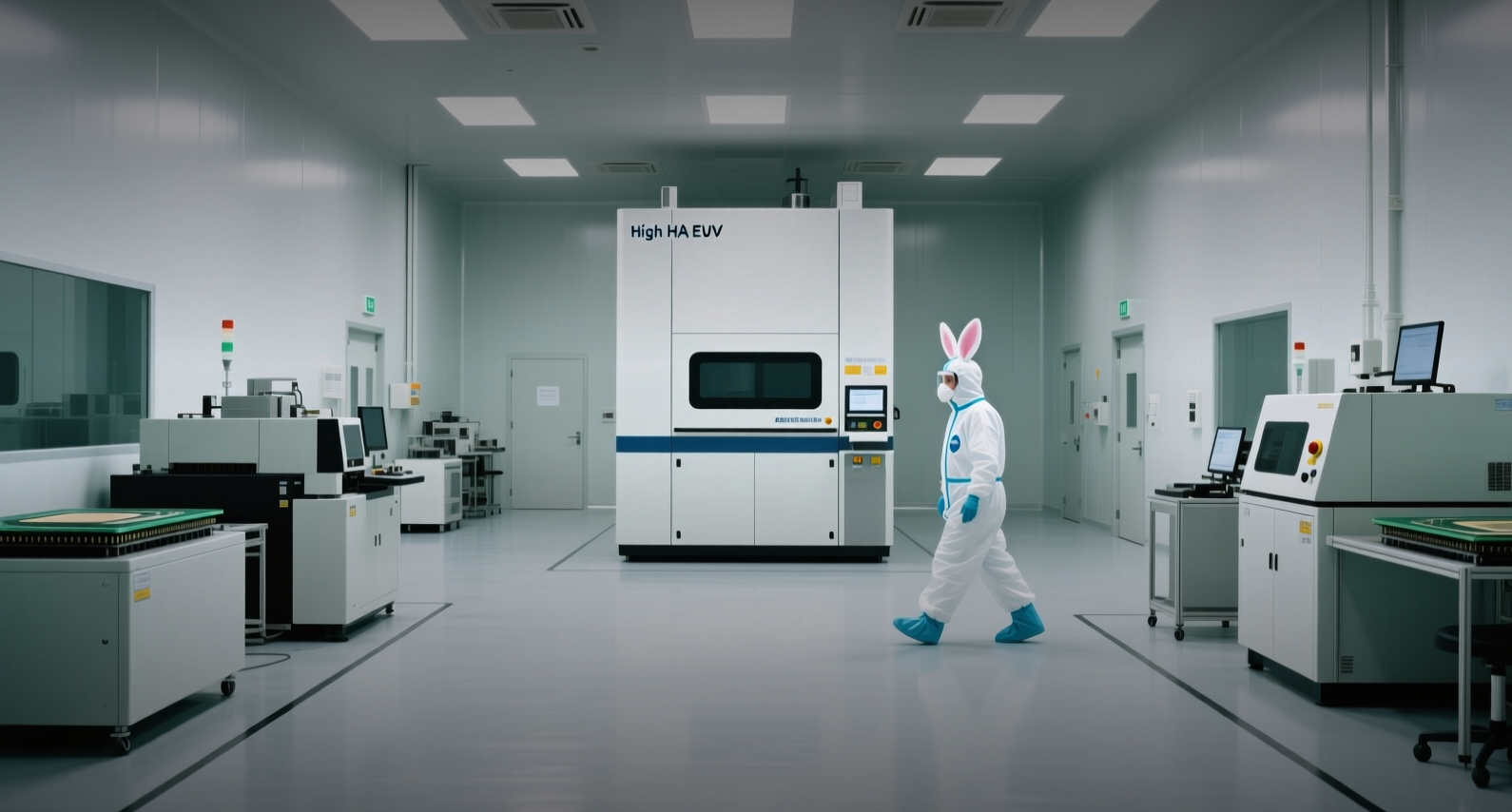
ASML and TSMC are pushing the semiconductor industry to adopt 12-inch photomasks for High NA EUV lithography, a shift that could lift scanner throughput by 40 percent and lower costs for AI-era chip production.
"High NA EUV adoption will ramp gradually along the device scaling roadmap, first using current 6-inch masks and then further supported by 12-inch masks, which enable greater scanner productivity," Christophe Fouquet, president and CEO of ASML, said.
TSMC intends to deploy High NA systems in high-volume manufacturing for advanced nodes starting in 2030, with a 12-inch mask pilot line targeted by 2031 and full lithography system readiness for production by 2033. Samsung Electronics plans to apply High NA EUV to memory mass production as early as 2028, while Intel has already taken delivery of the machines, which cost roughly $400 million each. The larger mask format eliminates stitching constraints — where circuits must be split and reconnected across mask boundaries — and could increase throughput from High NA tools by 40 percent, according to ASML Chief Technology Officer Marco Pieters.
The coordinated push locks in ASML's three largest customers — TSMC, Samsung and Intel — behind its High NA roadmap, with TSMC alone accounting for about 16 percent of ASML revenue. For chipmakers racing to meet AI-driven demand for advanced nodes, the transition addresses a bottleneck that has forced compromises in chip design and packaging.
Photomasks are precision templates that transfer circuit patterns onto silicon wafers during lithography. The industry has used 6-inch masks for decades, but as transistor architectures grow more complex — particularly for AI accelerators that require dense logic and memory integration — the smaller format forces chipmakers to stitch multiple mask fields together, adding cost and constraining design flexibility.
The move to 12-inch masks removes that constraint. Pieters said the larger format could increase throughput from High NA machines by 40 percent while simplifying the design process. That productivity gain is central to the economics of High NA EUV, which carries a price tag of roughly $400 million per system — a threshold that has made TSMC cautious about adoption until now.
TSMC Chairman and CEO C.C. Wei framed the initiative as a collective industry effort. "When the industry works together to solve complex problems, we unlock possibilities that no single company could achieve alone," he said.
The ASML-TSMC announcement on Sept. 7, made ahead of the SPIE BACUS Conference in Monterey, California, is not the only path to 12-inch masks. Samsung Electronics said it will join ASML's large-format mask consortium, while Intel has been contributing to the larger-mask push for more than three years through its own collaboration with ASML.
Samsung's position is distinct: it is the only global chipmaker operating both memory production and foundry services. The company plans to apply 12-inch photomask technology across future DRAM generations and logic foundry processes, with High NA EUV targeted for memory mass production in 2028. Samsung Vice Chairman and CEO Jun Young-hyun said the company will strengthen collaboration with ASML to lay the technology foundation for AI computing.
The convergence of three separate consortia around the same 12-inch standard matters for the broader supply chain. Mask suppliers, equipment vendors and materials companies will need to align their roadmaps to a single format transition, reducing fragmentation risk across the industry.
For ASML, the initiative removes a key adoption risk for its most expensive product line. High NA EUV systems represent the company's next growth engine after low NA EUV, which debuted in 2019. With TSMC — its largest customer at roughly 16 percent of revenue — now committed to High NA from 2030, and Samsung targeting 2028 for memory, the demand pipeline for these machines extends well into the next decade.
The 12-inch transition also has implications for chip economics. Larger masks mean fewer stitching steps, higher yield and lower per-chip costs — critical as AI workloads push transistor counts higher and packaging complexity grows. For Nvidia, AMD and other AI chip designers that rely on TSMC's advanced nodes, the shift could translate into more cost-effective future chip generations.
ASML shares rose 4.17 percent on the announcement, while TSMC gained 2.85 percent and Intel advanced 4.51 percent, according to Bloomberg data.
This article is for informational purposes only and does not constitute investment advice.
