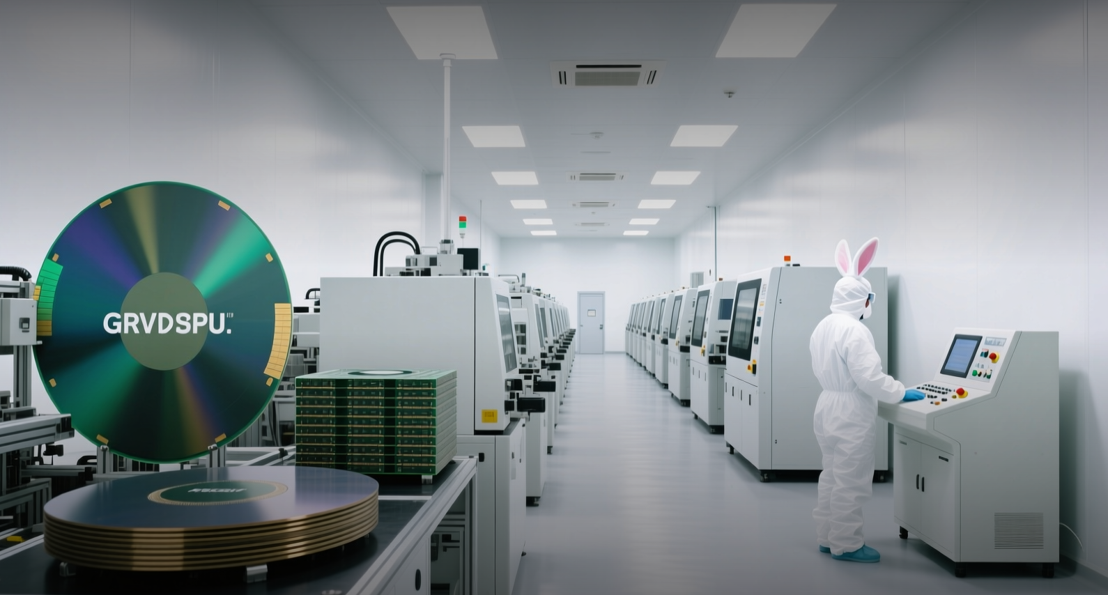
Samsung's three-phase HBM roadmap ends with zHBM, a design that stacks DRAM directly atop GPUs to cut memory power 70 percent.
Samsung's roadmap at Hot Chips 2026 repositions HBM's base die from a passive data relay into an active compute partner, culminating in zHBM — a 3D stack that cuts DRAM power 70 percent versus HBM5.
"By mastering advanced packaging and unified SoC-DRAM co-design, we will break through the power, area, and capacity bottlenecks constraining AI systems," Sangwook Han of Samsung's DRAM design team said.
HBM4 already exceeds 3 TB/s per stack, HBM4E pushes past 4 TB/s, and HBM5 doubles bandwidth with capacity above 60 GB. Samsung applied its D1c and 4nm logic processes to HBM4's base die, the first step toward merging DRAM with advanced logic.
The roadmap arrives as HBM spot prices have climbed about sevenfold and Micron and SK Hynix have sold out capacity through 2027, making memory the most expensive ingredient in AI server racks.
The base die becomes an intelligent partner
Today's HBM pairs a core die holding DRAM cells, stacked up to 16 layers, with a base die that handles control functions and talks to the GPU through a physical interface. Bandwidth scaling now hits two walls: the physical limits of through-silicon vias and the I/O ceiling inside the base die.
Samsung's first phase moves the memory controller off the GPU and onto a custom HBM base die. The controller occupies 5 to 10 percent of the compute chip's area, so offloading it frees space for extra cores and lifts performance 10 to 20 percent. A Heat Path Block built on the cHBM4 design cuts peak temperatures more than 35 percent and covers half the physical interface.
Phase two adds function to the freed space. Samsung plans to integrate memory expansion controllers and processing elements onto the base die, connecting LPDDR or additional HBM directly and offloading memory-bound attention computation from large language models. The company calls this AHBM.
zHBM eliminates the interposer
The third phase abandons the 2.5D interposer that sits GPUs and HBM side by side. zHBM stacks DRAM directly on top of the compute chip, using distributed I/O to shorten data paths and remove redundant modules such as SerDes. Samsung targets about 0.5 pJ/bit of I/O power, a 70 percent cut in total DRAM power, more than 100 W of savings per module, and 2.3 times the bandwidth of HBM4E.
The design requires wafer-on-wafer and hybrid copper bonding at sub-6-micron pitch, forcing DRAM and SoC teams to co-design from the start. Thermal limits currently point to about four stacked layers rather than 12 or 16, so engineering work remains.
Memory wall pressures the whole supply chain
Micron's HBM design architect Raghu Sriramaneni warned at the same conference that AI compute grows roughly threefold every two years while HBM bandwidth lags below twofold. In a package with two GPUs and eight 12-layer HBM4 stacks, memory occupies about 90 percent of the silicon — more than eight times the GPU area. Micron cited Meta's Llama 3 data showing about 17 percent of unplanned training interruptions traced to HBM.
SK Hynix, meanwhile, said its 16-layer HBM3E test chip thins each die about 10 percent versus 12-layer stacks, and that hybrid bonding becomes attractive around 20 layers. HBM production is inefficient: matching standard DRAM capacity takes about three times the wafer volume, per Micron.
The shortage is reshaping pricing across the stack. Deloitte estimates memory already represents about 25 percent of a high-end AI server rack's bill of materials, and Nvidia has told customers servers will cost more than 15 percent more from early next year. Micron, SK Hynix, and Samsung hold the pricing power, while Nvidia passes the bill to Microsoft, Alphabet, and Oracle. Samsung's zHBM, if it reaches production, would give the memory maker a structural cost edge over rivals — but the four-layer thermal ceiling and unproven hybrid bonding keep it years from the market.
This article is for informational purposes only and does not constitute investment advice.